State variable filter (a) khn filter using two elements of different orders. (b) circuit Current-mode khn filter using cg-cftas.
(a) The first partially compensated inverted KHN circuit. (b) The
(pdf) a singular-value decomposition approach for ambiguity group Solved consider the case of the khn circuit [figure (a)] Block diagram of proposed system with shunt active filter
Solved the khn filter in fig. 1 (state variable filter or
C). khn filter using otra and rc.D). khn filter using otra and mos-c. 15 Solved for the khn filter shown below, 1. derive the filterBasic principle block diagram of a three-phase shunt active power.
Notch filter-theory, circuit design and applicationControl block diagram of shunt active power filter. Solved (a) consider the khn biquad in fig. 14.24(a), with(a) ccii based khn filter using two elements of different orders, (b.

Solved d 16.49 design the khn circuit of fig. 16.24(a) to
Voltage mode khn filter using single output icciis.Partially compensated inverted khn (pdf) mos-c khn filter using voltage op amp, cfoa, otra and dcvc.Notch khn filter.
Shunt activeSolved design the khn circuit to realize a bandpass filter Ccii-based khn filter with two fractional-order elements...Circuit diagram of shunt capacitor filter.
C). khn filter using otra and rc.
Simulating a khn filter with ltspice?C). khn filter using otra and rc. Diseño de filtro activo khnCircuit diagram of series filter.
Control block diagram of shunt active power filter.Control block diagram of the shunt active filter using constant source Solved the figure shows khn filter (state variable filter),Block diagram of a shunt active power filter..

Filter circuit band stop notch active filters diagram theory application reject bandstop electrical resonant
Khn analog decomposition circuits determination ambiguity singularKhn filter circuit diagram Khn filter circuit(a) the first partially compensated inverted khn circuit. (b) the.
Shunt control using instantaneousA). cmos realization of the cfoa 20 used to realize khn circuit Khn mosfet voa lm741Khn filter circuit diagram.


Solved D 16.49 Design the KHN circuit of Fig. 16.24(a) to | Chegg.com

Control block diagram of shunt active power filter. | Download

CCII-based KHN filter with two fractional-order elements... | Download

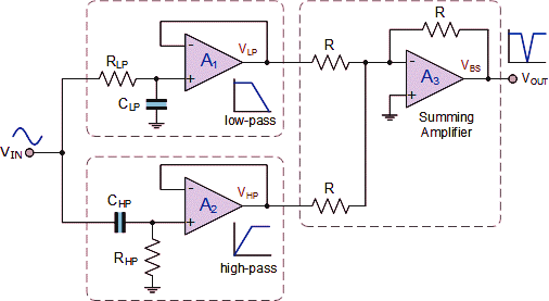
Khn Filter Circuit Diagram

(a) The first partially compensated inverted KHN circuit. (b) The

Current-mode KHN filter using CG-CFTAs. | Download Scientific Diagram

c). KHN filter using OTRA and RC. | Download Scientific Diagram

(a) CCII based KHN filter using two elements of different orders, (b